Buck Converter Basics: LM2596 Circuit Design Guide Inside!
Welcome to our comprehensive guide on Buck Converter Basics, where we dive into the world of efficient voltage regulation using the LM2596 circuit design! Whether you're an electronics enthusiast, a hobbyist, or a seasoned engineer, understanding the principles behind buck converters is essential for optimizing power management in your projects. In this post, we'll break down the fundamental concepts of buck converters, explore the features and benefits of the LM2596, and provide you with a detailed circuit design guide to help you implement this versatile component in your own applications. Get ready to enhance your knowledge and take your designs to the next level!
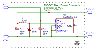
Lm2596 Dc Buck Converter Schematic Diagram
The LM2596 DC buck converter is a popular choice for efficient voltage regulation in various electronic applications, and understanding its schematic diagram is crucial for effective circuit design. At its core, the LM2596 operates by stepping down a higher input voltage to a lower output voltage, making it ideal for battery-powered devices and other low-voltage applications. The schematic typically includes essential components such as inductors, capacitors, and diodes, which work together to smooth out the output and minimize ripple. By analyzing the schematic, engineers can optimize parameters like switching frequency and output current, ensuring that the converter meets specific performance requirements. Whether you're a hobbyist or a seasoned designer, grasping the intricacies of the LM2596 schematic will empower you to create robust and efficient power supply solutions.
 www.circuitdiagram.co
 Lm2596 Buck Converter Circuit Diagram
In this section of our blog post, "Buck Converter Basics: LM2596 Circuit Design Guide Inside!", we delve into the essential components of the LM2596 buck converter circuit diagram. The LM2596 is a versatile and widely used step-down voltage regulator that efficiently converts a higher input voltage to a lower output voltage, making it ideal for various applications, from powering microcontrollers to charging batteries. The circuit diagram typically includes key elements such as the LM2596 chip, input and output capacitors, an inductor, and a diode, all of which work together to ensure stable voltage regulation and minimal ripple. Understanding the arrangement and function of these components is crucial for optimizing performance, improving efficiency, and enhancing the overall reliability of your power supply design. Whether you're a hobbyist or a seasoned engineer, mastering the LM2596 buck converter circuit will empower you to tackle a wide range of electronic projects with confidence.
 fixlibraryestaleirojg.z13.web.core.windows.net
 Lm2596 Buck Converter Circuit Diagram: A Comprehensive Guide
In this section of our blog post, "Buck Converter Basics: LM2596 Circuit Design Guide Inside!", we delve into the LM2596 buck converter circuit diagram, a crucial component for efficient voltage regulation in various applications. The LM2596 is a step-down voltage regulator that can deliver up to 3A of output current, making it ideal for powering devices that require a lower voltage from a higher voltage source. Our comprehensive guide will walk you through the essential elements of the circuit diagram, including the input and output capacitors, inductor selection, and feedback loop configuration. Whether you're a beginner or an experienced electronics enthusiast, understanding the LM2596 circuit design will empower you to create reliable power supply solutions for your projects. Join us as we break down the components and functionality of this versatile buck converter!
 www.queycomo.co
 Lm2596 Dc-dc Buck Converter Circuit Diagram
In the realm of power management, the LM2596 DC-DC buck converter stands out as a versatile and efficient solution for stepping down voltage levels. This circuit diagram showcases the essential components and layout required to implement the LM2596 in your projects. Typically, the circuit includes the LM2596 IC, input and output capacitors, an inductor, and a diode, all working together to convert a higher input voltage into a stable, lower output voltage. Understanding the intricacies of this circuit diagram is crucial for optimizing performance, ensuring minimal ripple, and achieving the desired output current. Whether you're designing a power supply for microcontrollers or battery-operated devices, mastering the LM2596 circuit design can significantly enhance your project's efficiency and reliability.
 wiringdiagramsuspiring.z14.web.core.windows.net
 Buck Converter Circuit Diagram Using Mosfet
You Might Also Like: Norovirus Stool Color How To Spot Signs
In our exploration of buck converters, the circuit diagram featuring a MOSFET plays a crucial role in efficiently stepping down voltage levels. The LM2596, a popular step-down voltage regulator, utilizes a MOSFET as a switching element to control the output voltage. In the circuit diagram, you'll notice the MOSFET is positioned between the input voltage source and the inductor, allowing it to rapidly switch on and off, thereby regulating the energy transferred to the load. This switching action minimizes power loss and enhances efficiency, making the LM2596 an ideal choice for various applications. Understanding the placement and functionality of the MOSFET within the buck converter circuit is essential for anyone looking to design or troubleshoot these power electronics systems effectively.
 schematicjakuleenazc.z13.web.core.windows.net